25% Less Energy: Micron's 2027 G11 NAND Cuts Power While Doubling Density
The memory maker plans to double storage capacity and cut power usage by more than 25% using a wafer bonding technique currently employed by few competitors.
By Jason Kovalenko ·
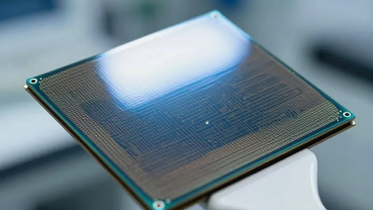
Memory manufacturers are under pressure to increase storage capacity while reducing the energy required to access data. Micron announced this week that its next-generation 3D NAND flash, designated G11, will begin high-volume production in the second half of 2027.
The company stated that G11 will achieve a storage density of approximately 42 gigabits per square millimeter in triple-level-cell form. This figure represents a near-doubling of the density found in the current G9 generation, which stands at roughly 21 gigabits per square millimeter. Micron also projects that input/output speeds will rise from 3,600 megatransfers per second to 5,400 megatransfers per second.
Energy efficiency is a primary driver for the new architecture. Micron said the energy used to transfer each bit of data will drop by more than 25%. These improvements aim to support high-capacity solid-state drives for client and data center applications, as well as specialized storage devices for artificial intelligence workloads that require higher bandwidth.
A central technical shift in G11 is the adoption of wafer-on-wafer bonding. This method allows the company to fabricate the memory array and the peripheral logic circuitry on separate wafers, each optimized for its specific function, before bonding them together. While Micron has used CMOS-under-array designs in previous generations, bonding provides greater flexibility in optimizing both the memory cells and the logic components independently.
Scott DeBoer, Micron’s president and chief technology and products officer, confirmed that the timing is right for this technology. He described G11 as the world’s most advanced NAND and noted that the design will move past 400 layers. Micron has not disclosed the exact layer count but stated that the design features an industry-leading memory cell pitch.
The company plans to share further technical details in 2027 as production approaches. Beyond G11, Micron said it is developing high-mobility materials and ultra-dense cell architectures to continue scaling in all three dimensions. DeBoer indicated that the roadmap focuses on new materials and densifying cell architecture without relying solely on increasing layer counts.